Norstan's Electrical Contact Manufacturing Blog
The Most Common Failure Scenarios for Electrical Contacts
Website Team
Often, when a product or component fails, it’s because it wasn’t adequately designed for the environment or the application in which it was used.
Think of the O-rings on the boosters of the Challenger Space Shuttle, which were never designed to survive a launch in cold weather. Or the Samsung Galaxy Note 7 smartphone, which had a tendency to catch fire because of poor design. Do you remember the infamous Ford Explorer from the last decade, which tended to roll over under certain conditions?
Electrical contacts are no different. If they’re not correctly engineered for the application and the environment in which they’re used, they won’t last long. What causes them to fail prematurely?
Here are some questions that will help you better understand the most common failure scenarios:
What is the current and voltage that will pass through the electrical contact? This must influence the size and material composition of your electrical contacts. Excessive current could cause the contact to weld closed or cause the contact to erode. If material cannot handle the current capacity for the application, erosion or welding will cause failure of the operating device.
Is there an arc generated when the switch opens or closes? If current is arcing across an electrical contact, it tends to clean the surface, helping to ensure excellent continuity. If there is no arcing, the contact is at the mercy of its materials, which may develop a contamination film or corrosion due to the environmental conditions to which the device is exposed.
How many cycles is the switch exposed to? If it must withstand a large number of cycles, the designer should choose a solid contact rivet or machine composite rivet for longevity.
How big is the package into which the switch will be incorporated? A common mistake made by many design engineers is making the package into which it’s being incorporated too small. The smaller the contact, the smaller it’s surface area. That makes it harder for the electrical contact to dissipate heat. Finally, the selection of materials can have a big impact on a device’s ability to dissipate heat. Certain metals cool faster than others.
What environmental conditions will the switch be exposed to? For example, you can’t use a copper contact in an application where the electrical contact will be exposed to air. When the surface of a copper contact oxidizes, it loses its ability to conduct electricity. Plating a copper contact with a metal that is resistant to corrosion can be an excellent, low-cost solution compared to using exotic, higher-cost materials.
Does the contact need to be wiped? Smaller electrical contacts are also prone to have problems operating consistently in temperature extremes, moist or dusty environments. In demanding applications like these, designers must design overtravel into the contact so it can be wiped clean during each cycle.
Get started: engineer electrical contacts that last
Norstan has an unparalleled depth of metallurgical and application knowledge that we can use to help you optimize the design of the electrical contacts in your switches. Have a metallurgical question? Ask Hugo
Norstan's Electrical Contact Manufacturing Blog

Key Factors When Choosing an Electrical Contact Supplier
Website Team
When it comes to electricity, a strong connection makes everything go. Current flows unimpeded, like a superhighway of electrons, and your machine works efficiently. It’s no different when you’re selecting an electrical contact supplier.
A partner with the right capabilities and qualities can energize your project and can result in a successful switch design. But the wrong supplier can be like a horrendous traffic jam – endless delays, questionable detours, application problems and even embarrassing failures.
#1 Metallurgical expertise
This is the most important quality of all.
Your ideal electrical contact supplier needs to have deep knowledge of theoretical and applied metallurgy, especially material qualities and limitations. Your supplier partner needs to anticipate how various metals and alloys will behave under a variety of conditions as an integral component in your products.
The supplier you select also needs to have a solid prototyping and testing process, because electrical contact design is equal parts art and science. In other words, the exact behavior of electrical contacts within a switch can only be discerned through sampling and testing. Your supplier should have a proven process for reaching the optimum contact design and material. It should meet your requirements and do so at a reasonable price.
Hugo Francisco, the president of Norstan, is one of the world’s leading experts on electrical contacts. His decades of knowledge and experience enable you to achieve the right solution for your application, while also avoiding pitfalls that could shorten contact life and cause premature switch failures.
#2 Electrical expertise
Ideally, your electrical contact supplier should have deep expertise in the electrical properties of metals, specifically:
- The levels of current and resistance that are required for the application,
- What device is connected to the electrical switch in which the contacts will be used? How much current will it draw?
- How arcing affects the life of electrical connectors
#3 Mechanical factors expertise
For best results, your electrical contact supplier must deeply understand the ways in which the shape and thickness of an electrical contact can affect its mechanical performance:
- The forces applied to it can also have a big impact on its durability.
- If an electrical contact opens and closes too slowly, it can weld shut.
- If it does so too quickly, the contact may shatter, accelerating material erosion and reducing contact life.
- If an electrical contact is subject to excessive vibration or heat, it could detach from its substrate, causing the switch to fail.
#4 Environmental factors expertise
Ideally, your electrical contact supplier needs to have a solid working knowledge of the environmental factors it will be exposed to, and how they are likely to impact electrical contact life:
- They need to plan for adequate heat dissipation in your switch design, because excess heat can shorten the life of your electrical contacts.
- If your switch application uses a non-arcing contact, then it’s at the mercy of the environment in which it’s used.
- If your switch uses a metal that oxidizes or sulfidates when exposed to moisture and other elements, it may interfere with the switch’s ability to make a reliable electrical connection.
#5 A keen eye for manufacturability
Your electrical contact supplier needs to be an effective partner, analyzing your switch designs with an eye toward manufacturability:
- Some materials and designs are easier to work with than others.
- An effective manufacturing partner should be able to help you work through design challenges and performance trade-offs.
- In other cases, the switch manufacturer needs to keep costs to a minimum. The electrical contact supplier can meet this need with a bimetal design. But this introduces new variables into its manufacturability and performance. Your electrical contact supplier should be aware of these pros and cons, and advise you accordingly.
For best results, your electrical contact supplier should also have extensive tooling and metal forming expertise in house. Why? Because many designs require multiple iterations to create a design that meets all of the mechanical and cost requirements of the project. Your supplier team should be able to iterate quickly – which can only happen if they have these capabilities in-house.
#6 Committed to a consultative relationship with you
Ultimately, your electrical contact supplier needs to be able to look at your switch design and ask the right questions about its application. From there, it needs to discern potential problem areas and help you tweak your designs to solve them. That requires in-depth knowledge of metallurgy, mechanical factors and other key disciplines that many suppliers don’t have. Their superficial knowledge means you take on greater risk. No one needs that!
Norstan has an unparalleled depth of metallurgical and application knowledge that we can use to help you optimize the design of the electrical contacts in your switches.
Ask Hugo A Question .
Norstan's Electrical Contact Manufacturing Blog
Auto-Wire & Tape Weld Electrical Contact Welding Process
Website Team
- TAPE WELD ASSEMBLY
- Mitsubishi Wire Cut System
- Model MV1200R
- Max Workpiece 810mm x 700mm x 215mm
- Max Wire Burn Area 400mm x 300mm x 215mm
- Max Taper Angle 15° Standard
- Ability to Burn up to 25° in Specific Conditions
- Wire Diameters .1mm – .3mm
- 4 Axis Capable
- Latest Wire Burn Technology
The auto-wire weld assembly process develops a metallurgical bond between the precious metal piece (wire) and Substrate (Terminal). The weld can be achieved horizontally or vertically. The amount of precious metal utilized for the finished good can be reduced significantly because overall contact height can be achieved by embossing the substrate (Terminal) to some specific thickness. The most critical limitation for wire weld assemblies is the contact size diameter. Also, only alloys, pure metal, and silver nickel manufacture by powder metallurgical process can be welded presently to substrates. No silver cadmium oxide or tin oxide materials. Set up times and production rates are excellent for quoting.
Tape weld assemblies also develop a metallurgical bond between tape weld projection and substrate (Terminal). Tapes can have various profile geometries to reduced significantly the amount of precious metal utilized for the finished good. The base material of the profile tape will have an integral impact on the ability of the device to dissipate heat thru the operating members. Profile tapes typically consist of a weldable section attached to the precious metal. Typically, the base of the tape consists of a low conductivity material like nickel-plated steel or copper alloys with very low conductivities. This is required to achieve the metallurgical bond between tape and substrates. The beauty of tape weld assemblies is the intriguing shape achieve to reduce the amount of precious metal such as gold and palladium alloy to almost a dot. The profile weld tape assemblies are widely used in an application where packaging is very small like telecommunication and medical application. Set up times and production rates are as good as those for wire weld assemblies.
Each specific project needs to be review with customers to determine the best course of action, by far wire weld and auto staking assemblies are the most cost-effective process, but the unique shapes for manufacturing profile tapes can provide sometimes significant advantages where packaging constraints requirements must be met.
Wire weld and Tape Weld Services At Norstan, we specialize in both wire weld and tape weld assemblies. With our knowledgeable and responsive team, we can help you with your application. Contact us about our wire weld and tape weld services today!
Norstan's Electrical Contact Manufacturing Blog
Benefits of Precision Stamping Custom Electrical Contacts
Website Team
Precision Metal Stamping
Metal stampers are using high-speed presses and stamping dies to form metal strip into more precise complete and semi-complete parts than ever before. New developments in precision metal stamping can quickly and accurately accomplish complicated stamping applications by using several drawing, folding, stamping, and piercing techniques to their advantage.
The Benefits of Precision Metal Stamping
Precision stamping comes with a host of unique benefits. This highly automated process reduces labor costs, especially as production volumes increase. This makes metal stamping the method of choice for producing large volumes of metal products.
Intricate Precision Metal Work
Advances in stamping technology have resulted in the growth of precision stamping, which can use tools to achieve highly accurate parts. This method is a great way to design:
- Sensitive automotive and aerospace engine components
- Aircraft navigation and radar equipment
- Machine Gears
- Surgical instruments
Many technological advances have improved the way metalworkers carry out precision stamping. Below are a few ways manufacturers now achieve higher levels of accuracy in their finished parts:
- Deep-draw stamping allow metalworkers to form 3D shapes like shells, squares, and cylinders
- Workers use the same die to perform in-die extrusion and tapping, eliminating the need for a weld nut secondary operations
- Progressive die design applies cutting-edge software to advance die creation
- Transfer stamping lowers costs and lessens secondary operations when stamping complicated geometries
Prototype Design
Many companies use metal stamping to carry out prototyping and testing. Computer-programmed stamping equipment can rapidly incorporate design changes into the product, allowing you to create several different variations of a part within 1–2-day turnarounds.
Types of Prototype Design
Progressive Strip Prototyping
A die guides the stock prototype material through the manufacturing process. Manual or automatic feeders move the work piece through each station, delivering a complete product at the end-stage. These automation capabilities mean that you can use progressive strip prototyping to make small parts to tight tolerances with quick turnarounds as there are much fewer opportunities for human error to occur during manufacturing.
Single-Part Transfer Prototyping
This process moves individual prototype parts manually from station to station. Each station either forms or blanks the piece according to programmed instructions. This method reduces tooling costs if the company maintains a standard design.
Metal Stamping at Norstan, Inc.
Norstan, Inc. continuously looks for new ways to improve and refine our processes and products. We also seek to implement the most sustainable manufacturing practices possible, working to reduce our energy usage and waste output.
If you would like to learn more about our precision metal stamping services, contact us today.
Norstan's Electrical Contact Manufacturing Blog
Surface Contamination and Electrical Contact Resistance
Website Team
Correlation of Surface Contamination Introduced by Feeding Equipment on Electrical Contact Resistance
Abstract
Contact degradation caused by austenitic stainless steel feeder bowls has raised concern among manufacturers of electrical contacts. The surface contamination of three contact materials fine silver, silver cadmium oxide (90%Ag 10%CdO) and a silver alloy (75%Ag 24.5%Cu 0.5%Ni) with 15 microinches (Ra) surface finish were investigated. Contact resistance probing was employed and surfaces were analyzed to explain the degradation process. The investigation elucidated the effects of various vibratory feeder bowl coatings which reduced surface contamination. The attainment of low contact resistance was explained as interactions among the nobility of contact material, type of coating and time spent in the vibratory feeder bowl.
1. Introduction
Austenitic stainless steel feeder bowls are the most used feeding equipment by manufacturers of electrical contacts in their assembly operations. Despite cleaning the vibratory feeder bowls after each production, some of the assemblies remained slightly contaminated. The presence of foreign matter on the surface of electrical contacts is usually the cause of high resistance failures. Electrical contact is a junction between two or more current-carrying members, which provides electrical continuity at their interface (1). Early research by various investigators has shown that the most common types of contaminations are oxides and corrosion products (2,3,4), particulate [5], wear and fretting [6), and contamination originating in the manufacturing processes.
In particular, feeding equipment (especially stainless steel feeder bowls), has been shown to enhance surface contamination and adversely affect contact resistance [9]. Contact assembly often introduces contaminants via force and abrasive friction into feeding equipment. The latter process can quickly introduce contaminant film, prohibiting metal to metal contact between the current-carrying members and degrading contact performance. Minute amounts of base metal are generated from the shank during feeding and become embedded in the contact faces. It is easy to remove loose particles or unoxidized oil films, but the removal of metallic inclusions or highly compacted particles is difficult indeed. Field data shown in Figure 1.1.1, from several electrical contact users, suggest the need to minimize contamination during assembly.
Various types of contamination have received attention throughout the years. However, very little experimental work has been done with coatings and fiber materials developed for vibratory feeder bowl applications. The coatings were chosen after recommendations from several feeder bowls and contact assembly manufacturers. This paper aims at discussing the correlation of surface contamination introduced by feeding equipment on electrical contact resistance.
2. Experimental Procedure
2.1 Experimental Conditions
Three commercially available coatings for vibratory feeder bowl applications were employed for the experiment. The coatings were brushlon, Teflon and urethane.
Brushlon is a unique combination of synthetic brush fibers with 20 degrees of tilt uniformly distributed in a flexible backing. To assure that contacts were in continual motion in the vibratory feeder bowl, twenty-degree sectors were cut and attached to the substrate with a sprayed adhesive.
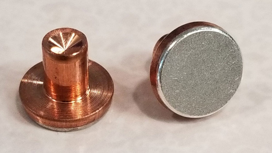
The contacts under consideration were rivets manufactured with radius head configuration, from the most widely used materials for electric contacts in the United States, as illustrated in Table I.
Contacts were manufactured under normal tool conditions and their surfaces contained spherical asperities from the tool surface. The surface finish of the test specimens was measured with a Mitutoyo surftest-201 surface measuring instrument. The arithmetic mean for the deviation of the departure of small scale surface irregularities from the mean line is called Ra.
Roughness measuring instruments which directly display RA are common and averaging the data minimizes the effect of scratches so that consistent results can be obtained. The approximate surface finish of contacts with radius head configuration was 15 microinches (Ra). A sample lot of fifty (50) contacts was submitted to coated vibratory feeder bowls for different intervals. Accelerated tests were performed to determine the interactions between coatings and contact materials. Once the contacts were in the vibratory feeder bowls for a prescribed time, the resistance of (7) contacts was measured employing an instrument called a contact resistance probe. The vibratory feeder bowls were cleaned with ethyl alcohol upon completion of the entire time cycle (360 minutes) before submitting new material to the test. A schematic diagram of the experimental flow chart is given in Figure 2.1.1.
2.2 Technique and Apparatus
Contact resistance was measured employing dry circuit techniques. The primary requirement for dry circuit testing of contacts has been previously described [9).
Figure 2.2.1 illustrates the contact resistance apparatus. The apparatus consists of fixtures for holding specimens of various sizes and shapes, and a Keithly 580 micro-ohm meter. A similar set up was used by Antler (10) and Nobel (11). A mechanism applies a measurable load which can be increased, decreased, or held constant. Only one contact spot was randomly assessed during testing. However, specific contact spots could be assessed employing the stage micrometers to move the probe holder. The reference surface (the probe) was manufactured from fine silver with a conical shape (gold diffused and gold treated).
The probe holder has been designed so force may be applied to the contact. An electrical load force gauge ACCU FORCE II is mounted on the top of the probe holder. A calibrated spindle on the side of the stage is advanced manually, while the electronic gauge displays the load applied to the sample. One of the micro-ohm meter voltage leads was attached to the probe holder and the other lead to the sample holder. A minimum of seven contacts from each interval was submitted to contact resistance probing. After each measurement, the probe was gently wiped with a tissue, assuring a debris-free surface similar to the technique used by Russell (12).
3. Experimental Results
3.1 Vibratory Feeder Bowls Coated With Brushlon Teflon and Urethane
As reported in a previous paper [9], contact resistance steadily increased as the time spent in the austenitic stainless steel vibratory feeder bowls increased, as a function of the material nobility. Contacts with various nobility levels and 15 microinches (Ra) surface finish were submitted to vibratory feeder bowls coated with (1) brushlon, (2) Teflon or (3) urethane 90 durometer and then subjected to contact resistance probing. The data represents rivets manufactured from fine silver, silver cadmium oxide (90Ag 10CdO) and a silver alloy (75AG 24.5Cu 0.5Ni) respectively.
Figure 3.1.1A depicts the resistance values of contacts submitted to a vibratory feeder bowl coated with brushlon. The interval values ranged from 15 minutes to 360 minutes. The three contact materials tested yielded average resistance readings, ranging from 1.1 milliohms after 15 minutes to 1.4 milliohms after 360 minutes at 100 grams load. Fine silver contacts manifested a gradual increase in contact resistance readings as the time spent in the vibratory feeder bowl increased
The Teflon coated vibratory feeder bowl also allowed attainment of low contact resistance. Fine silver and silver cadmium oxide (90Ag 10C1o) yielded the lowest contact resistance readings. The resistance readings ranged from 1.2 milliohms after 15 minutes to 1.0 milliohms after 360 minutes at 100 grams load. Silver cadmium oxide (90Ag 10CdO) produced very uniform resistance readings of 0.98 milliohms, as illustrated in Figure 3.1.1B. The resistance values of the silver alloy contacts gradually increased as a function of time spent in the vibratory feeder bowl.
Similar results were obtained for those contacts submitted to urethane-coated vibratory feeder bowls. Fine silver and silver cadmium oxide (90Ag 10CdO) produced the lowest resistance values of the three contact materials studied, as shown in Figure 3.1.1C.
Typical data distribution of the contact resistance readings is displayed in Figures 3.1.2A, 3.1.2B, and 3.1.2C. Scattering of the data was observed in some instances, due to test conditions and random formation of surface contamination on some contacts.
Figure 3.1.3 shows the average contact resistance and standard deviation of fine silver after spending one month in the coated vibratory feeder bowls. The graph in Figure 3.1.3 indicates that over time, the brushlon coating will rapidly degrade the surface and produce open circuit resistance. Teflon and urethane coatings yielded low contact.
Resistance values 2.0 milliohms and 1.5 milliohms respectively. The standard deviation was very narrow and (in some instances) there was no scattering of the contact resistance readings, as shown in Figure 3.1.3. On the other hand, fine silver contacts yielded open circuit resistance values after 45 minutes in the austenitic stainless steel vibratory feeder bowl [9].
surface, as shown in Figure 3.2.1D. Similar results were obtained for fine silver contacts after spending only 45 minutes in the austenitic stainless steel vibratory feeder bowl [9].
3.2 Scanning Electron Microscopy
Film contamination present on the surface of the contacts is shown in Figures 3.2.1 to 3.2.3. The contamination was evident after 6 hours in the coated vibratory feeder bowls for all contact materials studied. After spending one month in the coated vibratory feeder bowls, fine silver contacts were analyzed for contamination.
Specific attention was paid to the contaminant composition. The energy dispersion spectroscopy analysis was performed at an accelerating voltage of 10Kev. This provided minimal penetration of the electron beam and identification of typical contaminant material. Light elements such as carbon, oxygen, and nitrogen could be identified with the use of an ultra-thin window.
The analyses of the spot checks performed on the contacts surface reflected similar results. Isolated contamination was identified, and was comprised of hydrocarbon, as illustrated in Figure 3.2.1A, 3.2.1 B and 3.2.1C.
At one month in the brushlon coated vibratory feeder bowl, the fine silver contacts displayed a hydrocarbon film. The hydrocarbon film was thick and covered the entire contact surface, as shown in Figure 3.2.1D. Similar results were obtained for fine silver contacts after spending only 45 minutes in the austenitic stainless steel vibratory feeder bowl [9].
Minimal film contamination was detected on the contacts submitted to teflon coated vibratory feeder bowls. Only isolated fine dimple contamination was detected throughout the contact surfaces, as shown in Figures 3.2.2A, B and C. At one month in the teflon coated vibratory feeder bowl, an organic film (hydrocarbon) was detected on the contact surfaces. However, the film was thin and only the bottom of the contact apprentices was covered by contaminations as shown in Figure 3.2.2D.
The urethane-coated vibratory feeder bowl revealed similar film contamination, as was observed with the Teflon coating for the noble material tested. The population of the finely dispersed dimple contamination was limited and confined to the center of the contact as shown in Figure 3.2.3A and 3.2.3B. The silver alloy contact exhibited minimal surface contamination, as illustrated in Figure 3.2.3C. At one month in the urethane coated vibratory feeder bowl, the fine silver contacts exhibited surface conditions similar to the silver alloy contacts, as illustrated in Figure 3.2.3D.
4. Discussion
The severity of surface contamination produced by austenitic stainless steel vibratory feeder bowls as a function of material nobility has already been demonstrated.
The results suggest a general picture of the behavior of the contacts when subjected to coated vibratory feeder bowls. The contact materials fine silver, silver cadmium oxide (90Ag 10CdO) and a silver alloy (75AG 24.5Cu 0.5Ni) with 15 microinches (Ra) surface finish exhibited little surface degradation up to 360 minutes intervals. Low contact resistance was obtained for all contact materials tested, at 100 grams load and for every interval used in the investigation. This was an improvement over the results obtained during the investigation with austenitic stainless steel vibratory feeder bowls under the same test conditions.
Surface contamination is best understood when comparing the different coatings. Brushlon is a unique combination of synthetic brush fibers uniformly distributed in a flexible backing. In an industrial environment, lubricant mists adhere to the brush fibers. Therefore, contact surfaces become susceptible to film contamination independent of the silver content (nobility) of the materials. Low contact resistance was attained due to the isolated and random formation of the contaminant film on the contact surface.
Coatings such as Teflon and urethane cured to 85 durometers and 90 durometers produced very little surface degradation. The noble materials did not show susceptibility to film contamination. Substantially clean sites were available throughout the contact surface for assessment during contact resistance probing. The silver alloy (75AG 24.5Cu 0.5Ni) rivets achieved the cleanest surface in both coatings.
The Teflon and urethane coatings were effective in reducing film contamination. However, the addition of copper to silver increases resistance due to surface film oxidation. Therefore, slightly higher resistance values were obtained from the silver alloy than noble materials.
As shown in figure 3.1.3 surface degradation was evident as contacts spent one month in the brushlon coated vibratory feeder bowls. The film contamination covered the entire contact surface. Loads exceeding 500 grams were not sufficient to break the contaminant film to allow metal to metal contact. Contamination was present on the surface of contacts submitted to teflon coated vibratory feeder bowls; however, the contamination was not sufficient to cover contact asperities. Therefore, metal to metal contact was achieved very readily. Urethane was most effective in preventing film contamination. At one month in the vibratory feeder bowl, the contacts showed minimal surface contamination. We must note that (1) after one month, the teflon coating did wear; (2) contact wear was observed with the urethane coating; (3) surface finish was not altered after one month of exposure to teflon and urethane coatings; and (4) the energy dispersion spectroscopy analysis did not detect wear debris from the coatings embedded on the contact surface.
Clearly, it was shown that coated vibratory feeder bowls did not produce significant surface contamination, in comparison to austenitic stainless steel vibratory feeder bowls. When contacts were submitted to the same accelerated test in the austenitic stainless steel vibratory feeder bowls, an organic film consisting of hydrocarbon formed on the contact surface after 45 minutes. This was difficult to break even at 500 grams load and prohibited metal to metal contact. The silver alloy (75AG 24.5Cu 0.5Ni) rivets displayed similar contact resistance values after spending 120 minutes in the austenitic stainless steel feeder bowl and 360 minutes in the coated vibratory feeder bowls.
In summary, the results show that brushlon, teflon and urethane coatings prevented surface degradation. However, long term usage makes coatings susceptible to wear and the introduction of surface contamination is manifested again as was observed with austenitic stainless steel vibratory feeder bowls. Further study is needed to correlate the effects of long-term usage of coated vibratory feeder bowls on contact performance.
5. Conclusions
The effect of surface degradation by a brush fiber material and coated vibratory feeder bowls, on contact resistance of the three contact materials studied can be explained as follows:
- The coated vibratory feeder bowls, significantly reduced surface contamination compared to austenitic stainless steel vibratory feeder bowls under the same test conditions.
- The brush fiber material and coatings effectively reduced surface degradation. Low contact resistance was achieved, up to 6 hours regardless of the material.
- After one month, contacts submitted to brushlon coated vibratory feeder bowls exhibited identical film contamination as contacts submitted to austenitic stainless steel vibratory feeder bowls for 45 minutes.
- SEM analyses revealed little surface contamination and no wear debris on contacts submitted to teflon and urethane coated vibratory feeder bowls.
Norstan's Electrical Contact Manufacturing Blog
The Effect of Various Deburring Media Containing Mineral
Website Team
The Effect of Various Deburring Media Containing Mineral
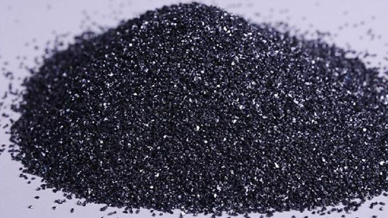
SILICON (SiO2) OR ALUMINUM OXIDE (A1,0.) ON CONTACT PERFORMANCE
Summary
Particle fragmentation and embedment of mineral silicon (SiO2) or aluminum oxide (A1,0,) introduced by deburring electrical contacts inhibit metallic conduction. The relationship between the concentration of mineral particles embedded on the rivet’s surface and contact performance was investigated. The fine silver rivets were tested in a dry circuit application and switched under various arcing properties to rate their performance.
The investigation elucidated that the attainment of low contact resistance in dry circuit applications was achieved independent of concentration and size of insulating particles embedded on the fine silver rivets at contact pressure less than 50 grams(0.5N). The contrary was observed when rivets were subjected to 12.5 VDC, 0.5 Amps and 2 Amps load. Degradation of the contact spot was directly related to the formation of a carbon film by absorption of organic vapor during switching, and not by decomposition of insulating particles (SiO, or Al2O2) on the rivets surfaces. The degradation process was significantly accelerated by varying arcing properties. The stable contact resistance obtained in dry circuit applications and erratic millivolt drop during electrical switching were explained as interactions among a concentration of insulating particles embedded on the fine silver rivets, particle size, and carbon film formed on the contact spot after switching.
- Introduction
Electrical contacts are subjected to numerous manufacturing steps, which can cause surface contamination. Rivets are polished to remove burrs and obtain smooth surfaces. To enhance the effect of this treatment, deburring media are utilized. A common source of contamination is mineral silicon used for deburring contacts after they have been fabricated. The presence of foreign matter on the surface of electrical contacts is usually the cause of high resistance failures. Electrical contact is a junction between two or more current-carrying members which provides electrical continuity at their interface [1]. Often, the rivets appear contaminated and no failure results, or on the open circuit the increased contact resistance is detected without any visible contact contamination.
The most common types of silicon compounds that have been found as constraints on contacts are organic silicon and organosilicon compounds and silicone. Early research by various investigators has shown many ways for silicone contamination to take place on electrical contacts resulting in detrimental effects on contact performance. Moberly [2], showed silicone transfer by vaporization when heating silicone oil to 200°C. Witter and Leiper [3], showed that silicone mineral contamination caused a significant increase in contact resistance, but did not cause loss of electrical continuity in devices operating at 1 newton of pressure and more than 100 volts. Trächslin (4), described finding silicate particles embedded on composite contact rivets from several contract manufacturers.
Trace contamination from base metals ordinarily would not cause low-level failure if contaminants remained pure metal. It is the subsequent change to insulating oxides or nitrides that ultimately prevents conduction. Loose particles or unoxidized oil films are easy to remove, but the removal of metallic inclusions or highly compacted/embedded particles from deburring media is difficult indeed.
The effects of surface contamination on electrical contacts have been studied for many years. However, prevention of surface contamination caused by deburring media containing mineral silicon (SiO2) and aluminum oxide (Al2O2), by manufacturers of electrical contacts seemed to be so obvious that papers on this subject could not be found. Embedment of particulate debris from the above process will degrade contact resistance and cause premature failure of the electrical contacts. The objective of this investigation is to further elucidate that even when rivets are contaminated with insulating particles, the driving force for degradation of the contact spot occurs only when an arc is sustained, due to absorption of organic vapors.
- Experimental Procedure
2.1 Experimental Conditions
The surfaces of the deburred rivets were subjected to quantitative surface analysis using Energy Dispersion Spectroscopy (EDS) techniques. Each contact was analyzed
The rivets under consideration were manufactured from fine silver (99.9% Ag) under normal tool conditions [15 microinches (Ra)]. They had radius head configuration and contained spherical asperities from the tool surface. The surface finish of test specimens was measured with a Mitutoyo Surftest-201 surface measuring instrument [5].
Once the rivets were manufactured with the desired surface characteristics, residual oils on the contact surface from the cold heading operation were removed by a conventional metal finishing process (burnishing). To assure that rivets were free from particulate debris, they were etched in a cyanide solution for 2 minutes or until a frosty appearance was visible.
The rivets were subdivided into smaller lots for contamination through tumbling with deburring media containing mineral silicon (SiO2) and aluminum oxide (Al2O2). The deburring process was performed with an open tumbler half-filled with deburring media and deionized water.
2.2
Chemical analysis of deburring media and rivets surface
The deburring media used in the investigation were crushed to develop fine powders (0.1 microns). These powders were then subjected to analysis using energy dispersion spectroscopy (EDS) techniques, utilizing an electron beam having an accelerating voltage of 5Kev. Table 2.2.1 depicts the quantitative results of analyzed powders in weight percent.
Rivets were deburred in an open tumbler half-filled with media containing various percentages of mineral silicon (SiO,) and aluminum oxide (A1,0z) and deionized water for 1 hour. They were then submitted to burnishing for 30 minutes.
The surfaces of the deburred rivets were subjected to quantitative surface analysis using Energy Dispersion Spectroscopy (EDS) techniques. Each contact was analyzed with an accelerating voltage of 10 Kev.
Each specimen was tilted 22 degrees and an acquisition time of 500 seconds was used. An area of approximately 1000 microns square near the center of each rivet was analyzed. This area best characterized the entire contact surface. The results of these analyses were quantified and approximate weight percent values were determined for aluminum oxide and mineral silicon as depicted in Table 2.2.2.
2.3 Technique and Apparatus
Contact resistance was measured employing dry circuit techniques. The primary requirement for dry circuit testing of contacts has been previously described [6]. Figure 2.3.1 illustrates the contact resistance apparatus. The apparatus consists of fixtures for holding specimens of various sizes and shapes, and a Keithly 580 micro-ohm meter. A similar set up was used by Antler [7] and Nobel [8]. A mechanism applies a measurable load which can be increased, decreased or held constant. Only one contact spot was randomly assessed during testing. However, specific contact spots could be assessed employing the stage micrometer to move the probe holder. The reference surface (the probe) was manufactured from fine silver with a conical shape (gold diffused and gold treated).
The probe holder has been designed so force may be applied to the contact. An electrical load force gauge ACCU FORCE II is mounted on the top of the probe holder, A calibrated spindle on the side of the stage is advanced manually, while the electronic gauge displays the load applied to the sample. One of the micro-ohm meter voltage leads was attached to the probe holder and the other lead to the sample holder. A minimum of seven rivets from each interval was submitted to contact resistance probing. After each measurement, the probe was gently wiped with tissue assuring a debris-free surface similar to the technique used by Russell [9].
2.4 Life Test
The various groups of rivets were tested in the experimental switching device shown in Figure 2.4.1. A power source allowed for adjustment of electrical parameters (500 Amps, 40 Volts max). The experimental switch gave cross-bar type make and break with closing force control by pre-adjusted terminals after assembly was completed. The operation parameters utilized in these tests were:
The experimental device was mounted on a rotary table, and cam-actuated, to push the plunger to open a set of contacts. Each device was actuated and deactivated at a rate of 16 times per minute. The electrical load for each pair of contacts was achieved by adjusting one wire wound 25 ohms resistor to obtain 0:50 amps and another 6.25 ohms resistor to obtain 2 amps resistance load and an open-circuit voltage of 12.5 volts DC. The voltage drop across the contacts was measured by using a digital voltmeter across the terminals. The circuit continuity after contact closure was monitored initially and after 10 and 10,000 cycles.
- Experimental Results
3.1 Effects of mineral silicon contaminated rivets on static contact resistance in dry circuit applications.
Figure 3.1.1 depicts in a graphical form the average static contact resistance of deburred rivets in various media. The static contact resistance values of the deburred and burnished rivets were compared to the contact resistance values of those rivets that were only burnished. The static contact resistance value yielded at 25 grams of contact pressure was 1.15 milliohms. When the contact pressure was increased to 50 grams, the static resistance value decreased to 0.94 milliohms. After rivets were deburred for 1 hour with the various media, the static contact resistance values yielded for test conditions 2 through 5 were 1.32, 1.08, 1.13 and 1.19 milliohms. At 50 grams of contact pressure, the static contact resistance values yielded were 1.05, 0.91, 1.00 and 0.97 milliohms respectively.
The cause for such negligible static contact resistance is best explained by the surface analysis of the deburred rivets. Figure 3.1.2 depicts the typical sizes and concentration of fragmented deburring media embedded on the rivet’s surface. The 1000 microns square examined near the center of the rivet revealed insulating particles scattered throughout the area. The insulating particles embedded on the rivet’s surface were approximately 0.25 microns in diameter.
A graphical representation of the average millivolt drop is depicted in Figures 3.2.1A and 3.2.1B. The device was actuated at 0.5 amps or 2 amps at 12.5 VDC. The millivolt drop measured initially and after 10 cycles ranged from 4 milliohms to 10 milliohms respectively. The contact spot degradation was directly related to the arcing properties and number of operations used. After 10,000 operations the millivolt drop for the various conditions tested ranged from 200 millivolts to 500 millivolts, as illustrated in Figure 3.2.1A. Actuating the device with 2 amps of load yielded 18 millivolt drop initially for all test conditions and after 10 cycles ranged from 25 millivolts to 40 millivolts respectively. The millivolt yield after 10,000 cycles ranged from 150 to 200 millivolts for the various test conditions investigated, as illustrated in Figure 3.2.1B.
The contact spots of the rivets from selected test conditions were analyzed by energy dispersion spectroscopy (EDS) for carbon and mineral silicon. The peak ratio of carbon and relative weight percent of mineral silicon and aluminum oxide are depicted in Figures 3.2.2A and 3.2.2B. When the device was actuated with 0.5 amps, the carbon present in the contact spot was 0.063 peak percent for all test conditions. The concentrations of mineral silicon and aluminum oxide ranged from 0.2 to 0.58 and 0.0 to 0.2 weight percent, as illustrated in Figure 3.2.2A. As expected, mineral silicon and aluminum oxide were not detected in test condition 5. Increasing the load to 2 amps allowed for a substantial increase in the carbon formation on the contact spot. The carbon peak ratio increased to 0.125% as illustrated in Figure 3.2.2B. The mineral silicon and aluminum oxide at the contact spot remained exactly the same as the devices actuated with 0.5 amps.
3.3 Scanning Electron Microscope Examination
Energy Dispersion Spectroscopy (EDS) was performed at an acceleration voltage of 10 Kev. This provided identification of typical contaminant material. Light elements such as carbon, oxygen, and nitrogen could be identified with the use of an ultra-thin window.
Figures 3.3.1 A, 3.3.1 B, 3.3.1 C, and 3.3.1 D depict scanning electron microscope photographs of the contact spot after actuating the device at 0.5 amps and 2 amps. The contact spot exhibited a gradual increase in carbon formation directly related to the arcing properties used. Figures 3.3.2 A, 3.3.2 B, 3.3.2 C, and 3.3.2 D depict the contact spot after ultrasonic cleaning with acetone. The surface of the contact spot revealed some remaining carbon and very fine fragments of the insulating particles embedded on the surface. These mineral particles were observed on rivets in test condition 2 regardless of the arcing properties used, as illustrated in Figures 3.3.2 A and 3.3.2 B. The contact spot of rivets from test condition 5 did not exhibit any mineral silicon or aluminum oxide on its surface, as expected. Only scattered carbon debris was detected as illustrated in Figures 3.3.2 C and 3.3.2 D. The surface analysis of rivets from test condition 4 revealed identical surface morphology as observed in those rivets from test condition 2.
4. Discussion
The results illustrated the behavior of the contacts when subjected to dry circuit applications or actuated with various arcing properties. The rivets tested in dry circuit applications attained low static contact resistance very readily. In fact, those rivets purposely contaminated with the various deburring media containing different concentrations of mineral silicon and aluminum oxide yielded identical static contact resistance values compared to those rivets manufactured and burnished in the appropriate solution.
In dry circuit applications, the most important factor contributing to the attainment of low static contact resistance is a clean contact surface. Although the surface of the rivets was contaminated with deburring media containing mineral silicon and aluminum oxide in various concentrations, the fragmented particles were scattered throughout the rivet’s surface as indicated in Figure 3.1.2. The actual fragmentation of the deburring media was 0.25 microns in diameter and very similar in all conditions tested. The latter condition allowed for the attainment of low static contact resistance regardless of the concentration of mineral silicon and aluminum oxide in the deburring media employed.
The initial electrical switching of the contacts produced insignificant millivolt drop but increased when tested under the various arcing properties. The contact spot progressively degraded as the number of operations increased to 10,000 cycles. Degradation of the contact spot was greatly influenced by the arcing properties used. As the current increased from 0.5 amps to 2 amps, the contact spot revealed evidence of some cleaning of the carbon film. Although the carbon film was slightly broken by subsequent arcing striking the rivet’s surface, the remaining carbon film adhered to the contact spot prohibiting metal to metal conduction. As a result, the millivolt drop measured at the end of 10,000 operations was considered an open circuit for both cases. However, the scanning electron microscope revealed that the concentration by weight percent of insulating particles presents on the contact spot prior to and after electrical switching was identical. This indicated that absorption of organic vapor during arcing produced the carbon film which adhered to the contact spot, instead of decomposition of the deburring media.
5. Conclusions
The effect of rivets contaminated with deburring media containing various concentrations of mineral silicon and aluminum oxide on dry circuit applications and degradation of contact spot during switching can be explained as follows:
The attainment of low static contact resistance was achieved in dry circuit applications regardless of the concentration of mineral silicon and aluminum oxide embedded on the rivet’s surface at contact pressure less than 50 grams.
During switching contact spot degradation was the result of absorption of organic vapor which formed carbon on the contact surface, instead of decomposition of the deburring media embedded on the rivet surface with subsequent arcing.
Degradation of the contact spot was accelerated by increasing the current from 0.5 amps to 2 amps and the number of cycles to 10,000.
Scanning electron microscopic examination revealed that insulating particles embedded on the rivet’s surface were approximately 0.25 microns in diameter and the concentration by weight percent was identical prior to and after actuating the device.
Norstan's Electrical Contact Manufacturing Blog
Everything You Need To Know About Electrical Contacts
Website Team
Electrical contact or connection failure can spell disaster for your facility or appliance’s operations. Issues with these systems can cause costly damage to capital equipment, not to mention injury or loss of life. Maintaining well-functioning electrical contacts is an important element to ensuring the performance and safety of your electronic equipment and components.
An electrical contact a switch that uses a secondary, low-voltage power source to complete or interrupt circuits that affect an electrical current. Unlike relays, they carry higher circuit loads and connect directly to high-voltage feeds, and they don’t interrupt short circuits like circuit breakers.
Electrical contacts consist of three basic parts:
- Operating coil
- Stationary contact
- Movable contact
By sending low-voltage power through the coil, the electromagnetic current activates the movable contact to open (thereby interrupting current flow) or close (thereby completing the circuit) against the stationary contact.
Electrical contacts are common in electrical mechanical devices that operate with a broad range of voltages and functions. Some of their most important uses include in:
- Household appliances
- Motors
- Control centers
- Power plants
- Assembly lines
- Presses
- Conveyors
- Cranes
These specialized switches come in two different contact states: normally closed (NC) and normally open (NO).
Electrical Contact States
Depending upon the specifics of applications that use electrical contacts, either a normally closed or normally open contact will be installed. It’s important to know the difference between each type of system so you can determine the correct choice for your application.
- Normally open switches default in the open position, meaning that no electrical current runs through them unless operators or processes close the circuit. Examples of normally open circuits include lighting occupancy sensors, equipment cooling systems, and pilot lights.
- Normally closed switches default in the closed position, meaning that an electrical current runs through them unless operators or processes open the circuit. Examples of normally closed circuits include emergency shutoff buttons, pump shutoff buttons, overheating/tip over switches, and shutoff bars.
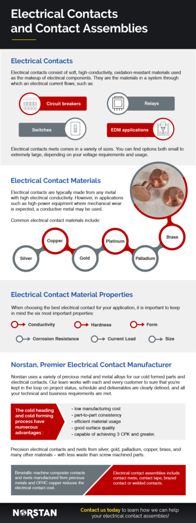
Common Metals Used to Create Electrical Contacts
Building properly functioning electrical contacts requires the use of materials with:
- Good conductivity
- Resistance against oxidation, corrosion, and mechanical wear
- Cost efficiency
- Application-specific properties
Among the common metals used to create electrical contacts are:
- Silver
- Copper
- Gold
- Platinum
- Palladium
- Brass
Each of these metals has essential properties that make it a proper fit for various electrical contact installation types and functions.
How to Choose the Right Electrical Contact for Your Application
Choosing the right electrical contact for your application will significantly improve its reliability and performance within the system.
There are six essential properties to consider when making this choice:
1. Conductivity: This measures a metal’s ability to resist or conduct electric currents as specified by the International Annealed Copper Standard (IACS); in this system, copper establishes the baseline at 100% conductivity, and other metals are rated in accordance to their capacities
2. Corrosion resistance: This relates to the ability of the contacts to resist chemically induced corrosion over time
3. Hardness: This evaluates four resistance or deformation factors under applied pressure, including:
- Ductility
- Elasticity
- Plasticity
- Tensile strength
4. Current load: This refers to the maximum current load capacity of the material
5. Form: This specifies the various shaping capacities of the material for its specific application
6. Size: This measures the length, width, and thickness of the material or its outside diameter in relation to its application
How to Reduce Electrical Contact Resistance
Bad electrical contacts or electrical contact failure affects both the performance and safety of the components and systems they serve. Contact failure increases the resistance of the conductor and prevents proper current flow.
Corroded battery cables on an automobile are a common example of electrical contact failure, which can lead to a breakdown in vehicle performance. In critical cases, electrical contact resistance causes overheating or cooling failures that can result in explosions, which compromise the safety and security of operators and the facility as a whole.
Reducing contact resistance starts with choosing the proper electrical contact material according to the six essential steps provided above, periodically inspecting and replacing worn contacts, or cleaning and maintaining corroded electrical contacts.
How to Clean Electrical Contacts
Operators must regularly clean electrical contacts to reduce their contact resistance and ensure good operational safety and performance. Many electrical contacts can be cleaned using common household items by following these steps:
- Disconnect main power source and any low-voltage auxiliary power
- Access the electrical contacts
- Wipe away loose corrosion with a clean cloth
- Dip a cotton swab in distilled white vinegar and apply the solution directly to the corroded contacts
- Wipe off liquefied corrosion and repeat step 4 if necessary
- Create a paste that consists of two parts sodium bicarbonate (baking soda) and one part water
- Apply this paste to corroded contacts and allow it to dry
- Wipe away the dried paste and corrosion and repeat step 7 if necessary
- After ensuring that there is no further corrosion, remove all paste and liquid from the contacts
- Reassemble and reconnect power sources
While cleaning oxidation and corrosion from contacts, be sure to inspect the various elements of the system for weakness or wear. Replacing electrical contacts before they wear out, become too resistant to electricity, or fail completely results in significantly improved cost savings and security advantages.
Norstan, Your Electrical Contact Supplier
Norstan is a leading manufacturer of highly specialized precision electrical contacts. Our products operate within a wide variety of applications, including:
- Vehicles
- Appliances
- Elevator control systems
- Aerospace systems and components
We’re also a leading OEM and supplier of electrical parts across a broad range of industries. From our Wisconsin facility, we produce:
- Bimetallic machine composite contacts and rivets from precious metals bonded to OFHC copper
- Electrical contact assemblies with rivets, contact tape and brazed or welded contacts
- Eectrical contacts made of silver, gold, palladium, copper, brass, and other highly conductive materials that generate less waste than screw-type machined components
Our team members strive to ensure that every customer remains up to date on project status, schedule, and delivery, and we constantly strive to meet or exceed your technical and organizational requirements. Norstan’s cold forming processes yield a number of benefits for our clients, including:
- Low manufacturing costs
- Part-to-part consistency
- Efficient material usage
- Optimal surface quality
- Capacity to achieve 3 CPK and greater
We’ve applied more than 50 years of experience toward producing the highest-quality products at the most competitive prices available in the industry. We also rely on our excellent customer service and sales representatives to help develop custom solutions that match your unique needs. Production of our electrical contacts occurs in an ISO:9001-registered facility with a commitment to providing a complete, cost-effective solution for our clients.
Electrical contacts are a vital element in ensuring the performance and safety of electromechanical devices and systems.
Contact us to learn more about how Norstan can help you improve or maintain your electrical systems.
Norstan's Electrical Contact Manufacturing Blog
Differences Between Spot Welding & Projection Welding
Website Team

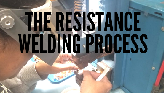
The resistance welding process is commonly utilized in budget projects because it requires no additional materials outside of the metal that’s being joined.
Fortunately, the cost-effective nature of the process doesn’t translate to a less reliable weld. While differing welding methods vary in cost, the appropriate method is largely chosen by what is best suitable for the application.
Each type of welding has merit for particular types of jobs, including resistance welding.
Norstan offers our clients two varieties of resistance welding: spot and projection welding.
Projection welding is actually a modification of spot welding, the pioneer resistance welding process. Projection welding is generally used for projects with thicker materials (around 0.035” and thicker).
While it can be also used to join thinner metal pieces together, that tends to be a job left for spot welding.
Spot Welding
Spot welding typically joins metal sheets. It’s one of the oldest welding practices still in use today.
Using electrodes with pointed tips to create opposing forces allows pieces of metal to be heated and subsequently joined with ease.
The electrode shape used in this process determines the various weld factors, such as:
- Current
- Heat generation
- Weld nugget size
The automotive industry relies heavily on spot welding when it comes time to join segments of automobile bodies and other large components. Other large items, such as household furniture and other domestic appliances and equipment are also frequently assembled using spot welding.
Spot welding is ideal for applications utilizing carbon steel and aluminum. In some cases, stainless steels, nickel alloys, and titanium can also be spot welded. The process also lends itself well to automation, which is seen as a notable benefit for many fabricators. Robots and manipulation systems can easily be programmed to perform spot welds.
The spot welding process offers manufacturers a range of advantages, including:
- Affordability
- Speed
- Efficiency
- Easily automated
- Sheets as thin as 0.25” can be spot welded without issue
Projection Welding
Like spot welding, the projection welding process relies on heat generated by an electric current to join metal pieces together. Projection electrodes are capable of carrying more current than spot welding electrodes and can, therefore, weld much thicker materials.
During the projection welding process, two flat electrodes cover the face of a fastener. The projections themselves absorb and disperse heat, which allows strong welds with exceptional aesthetics to be produced.
Even contact and pressure between the fastener’s projections and the base metal helps avoid excessive electrode pressure.
The projection welding process is ideal for joining together metal components with embossments. It’s frequently utilized in electrical, automotive, and construction applications, in part due to the strength of the welds it creates.
Projection welding offers benefits such as:
- A superior heat balance compared to other resistance welding methods
- Ideal for scenarios requiring thick pieces of metal to be joined together
Welding Services at Norstan
Norstan offers clients both spot and projection welding services tailored to meet their individual needs. Our resistance welding services are ideal for those in the automotive, aerospace, and manufacturing industries, but can benefit any organization in need of strong welds.
Our team specializes in both spot and projection welding. With our knowledgeable, responsive staff at your side as you embark on your project, you’ll never need to worry about the quality of the parts or service you’ll receive. We’re fully committed to providing 100% customer satisfaction through innovative and attentive work.
A member of our team will be glad to speak with you about the specific requirements of your industry or application.
From there, we’ll work towards building an affordable, forward-thinking, and effective solution tailored to your project. If you’re interested in learning more about Norstan’s welding services, contact us today.
Norstan's Electrical Contact Manufacturing Blog
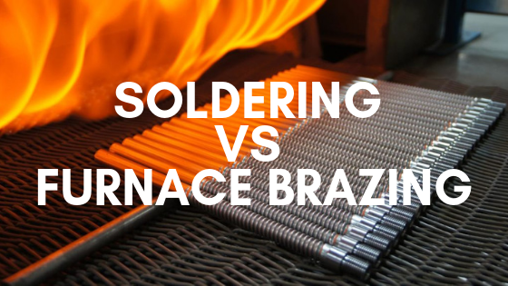
Differences Between Soldering & Furnace Brazing Contacts
Website Team
What’s the Difference Between Soldering and Furnace Brazing?
Furnace brazing joins metals by melting a filler metal developing a metallurgical bond between substrates. This process works well in mass production applications because it produces strong joins without requiring a high degree of precision. It is also very flexible.
The metallurgical bond developed between substrates has a tensile strength higher than the substrates. The metallurgical bond developed between substrates has a tensile strength higher than either substrate being joined together. This strong bond allows for higher current carrying capacity applications.
Furnace brazing operates with different types of furnaces:
- Controlled atmosphere furnaces
- Continuous or mesh belt furnaces
Norstan specializes in furnace brazing, which we believe achieves the strongest welds in the most cost-effective manner.
Soldering vs. Furnace Brazing
Furnace brazing operates similarly to soldering. Both joining types use filler metals to create the metallurgical bond between workpieces together, which allows for increased versatility and ease of use. However, a few key differences distinguish these techniques from each other.
Each technique uses different filler material. Soldering typically operates at much lower temperatures than brazing, using fillers that melt at or below 840°F (450°C). Therefore, soldering primarily works with gold, silver, copper, brass, iron, and other soft metals.
Because they possess lower melting points, soldered metals’ bonds aren’t as strong as those of as brazed or welded metals. Therefore, soldering is great for creating precision welds in applications with sensitive environments, such as electronics or medical devices. But furnace brazing creates durable welds at higher production volumes and with stronger metals.
Furnace Brazing Creates Stronger Welds
The American Welding Society (AWS) defines furnace brazing as welding that operates with filler metals with melting points higher than 842°F (450°C). Brazing also requires the use of a protective atmosphere to reduce the risk of impurities negatively affecting the bond.
Furnace brazing can take place in either flux or vacuum environments, and it develops stronger bonds than soldering. Brazed joints have shear strength five times as strong as that of soldered joints.
Brazing also allows for the use of a wide variety of filler metals, such as:
- Aluminum-silicon alloy
- Copper
- Copper alloys with silver, zinc, and tin
- Gold alloys
- Silver
- Silver alloys
- Nickel alloys
- Amorphous brazing foil
Welders often prize brazing specifically for its efficiency and reliability. Because it operates in environments with no airborne particles or contamination, brazing creates extremely clean welds and prevents impurities from affecting the metals.
Additionally, brazing mitigates many of the difficulties of working with flux, such as corrosion, excess porosity, crack formation, weld deformation, slag inclusions, irregular wire feed, and high levels of smoke and fumes. Flux-free braze joints tend to feature increased strength and integrity.
Furnace Brazing at Norstan
Ultimately, choosing between brazing and soldering depends on what metals you want to join, where they’re located, and whether you want to work with flux. Some systems, like HVAC systems, rely on smooth, clean welds, rendering excess flux residue problematic.
With a 100% satisfaction guarantee and an innovative, knowledgeable, and responsive team, Norstan can help you make the right call for your situation. Reach out to us today to request a free quote, and let’s help you ace your next welding project.
Norstan's Electrical Contact Manufacturing Blog

How to Find a Reliable Custom Electrical Contact Supplier
Website Team
Imagine if your automobile had rope steering, like an old-fashioned go kart. You could steer it, but not very accurately. Chances are, you’d be running into things and endangering other drivers. That’s what it’s like when you’re trying to work with an electrical contact supplier that has limited product knowledge. You’ll get to your destination – a finished parts order – but the journey is likely to be painful.
Norstan’s engineering team can make material and geometry recommendations for electrical contacts to meet specific application needs is as much art as it is science. It often requires iterative testing and sampling to zero in on a solution that does the best job of meeting the performance and life cycle needs of the switch it works within.
Over time, engineers develop a deep knowledge of what works and what doesn’t. They’re able to look at a design challenge and say, “I’ve seen this issue before. I know what to do to solve it.” Having this application knowledge in-house enables your electrical contact supplier to iterate to a final solution faster than if they rely on an outside partner for that expertise.
An electrical contact supplier with in-house tooling expertise is also able to respond faster to your needs. All communication happens within the company, ensuring that you get prompt answers to your questions. Passing your questions and requests via a third-party firm increases the odds of miscommunication. It can also slow project execution, because your requests need to be queued within two sets of production backlogs, not just one.
When problems do occur, an electrical contact supplier with in-house tooling expertise can respond and fix problems quickly, increasing the odds that you’ll get your parts on schedule with fewer production hiccups.
Machine tools are precision devices that must be rigorously maintained to ensure the components they produce for you are of consistently high quality. Your supplier is more likely to ensure that their machine tools are well maintained than your supplier’s supplier.
Finally, the components you order from an electrical contact supplier with in-house tooling expertise are likely to be more affordable than those produced by a third party. Each company in the supply chain must make a profit. It stands to reason that if you can minimize the number of parties involved, the more affordable the parts will be.
Norstan’s in-house tooling staff averages over 20 years of experience, ensuring that your electrical contact designs will be optimized and built efficiently and cost-effectively. Most of its competitors rely on external shops for machine tooling, which means they can’t be as responsive and affordable as Norstan.
When it has to be right, count on Norstan to deliver premium-quality electrical contact solutions.